This article will give out a brief introduction to basic concepts in AMD GPU. Its user-level APIs are similar to CUDA, for example, runtime sync API, with only the replacement of cuda to hip. But for underlying ISA and hardware components, there exist some obvious differences between NVIDIA and AMD.
Architecture Codename
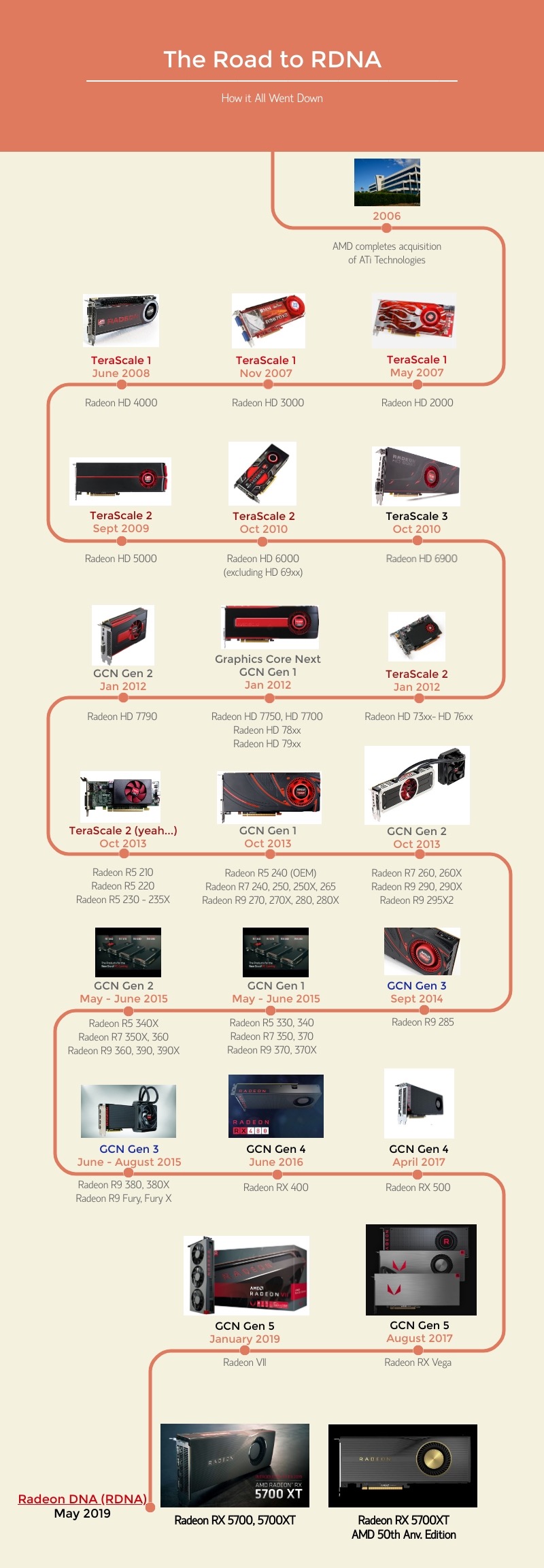
The above figure borrowed from r/amd demonstrates the timeline of AMD GPUs since the ATI acquisition. From it, we can see RDNA is the successor of GCN architecture, while at the beginning, the mainstream codename is TeraScale. And one architecture codename usually matures several generations of GPU products, for example, the GCN architecture includes five generations and comprises Polaris and Vega families, where the former targets low- and middle-end markets, and the latter aims at professional graphic users.
AMD Intrinsic is its professional brand for the datacenter market, whose main competitors are the NVIDIA Tesla series and Intel Xeon Phi GPUs. It’s also called CDNA architecture.
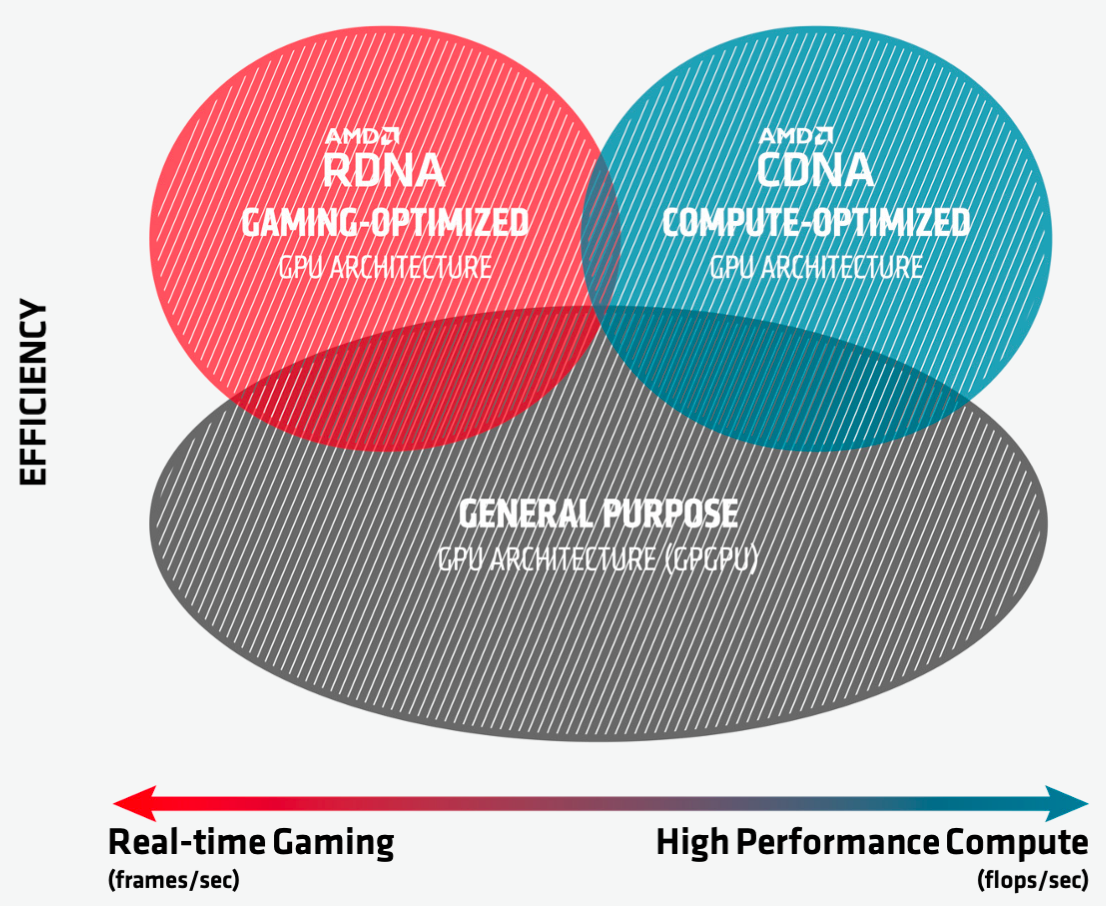
This figure (from AMD CDNA white paper) shows the comparison between the two AMD GPU brands, where RDNA emphasizes real-time gaming rendering in the gaming field, while CDNA is focusing on the floating-point performance required by HPC and AI workloads.
There is another subtle concept in AMD GPU: gfx, for example, the Navi 21 generation Radeon RX 6900 XT belongs to the gfx10.3 (sometimes gfx1030) family. In my point of view, the gfx is an analog concept with NVIDIA’s compute capability (CC), e.g., the NVIDIA A100 GPU has CC = sm80.
AMD GPU Concepts
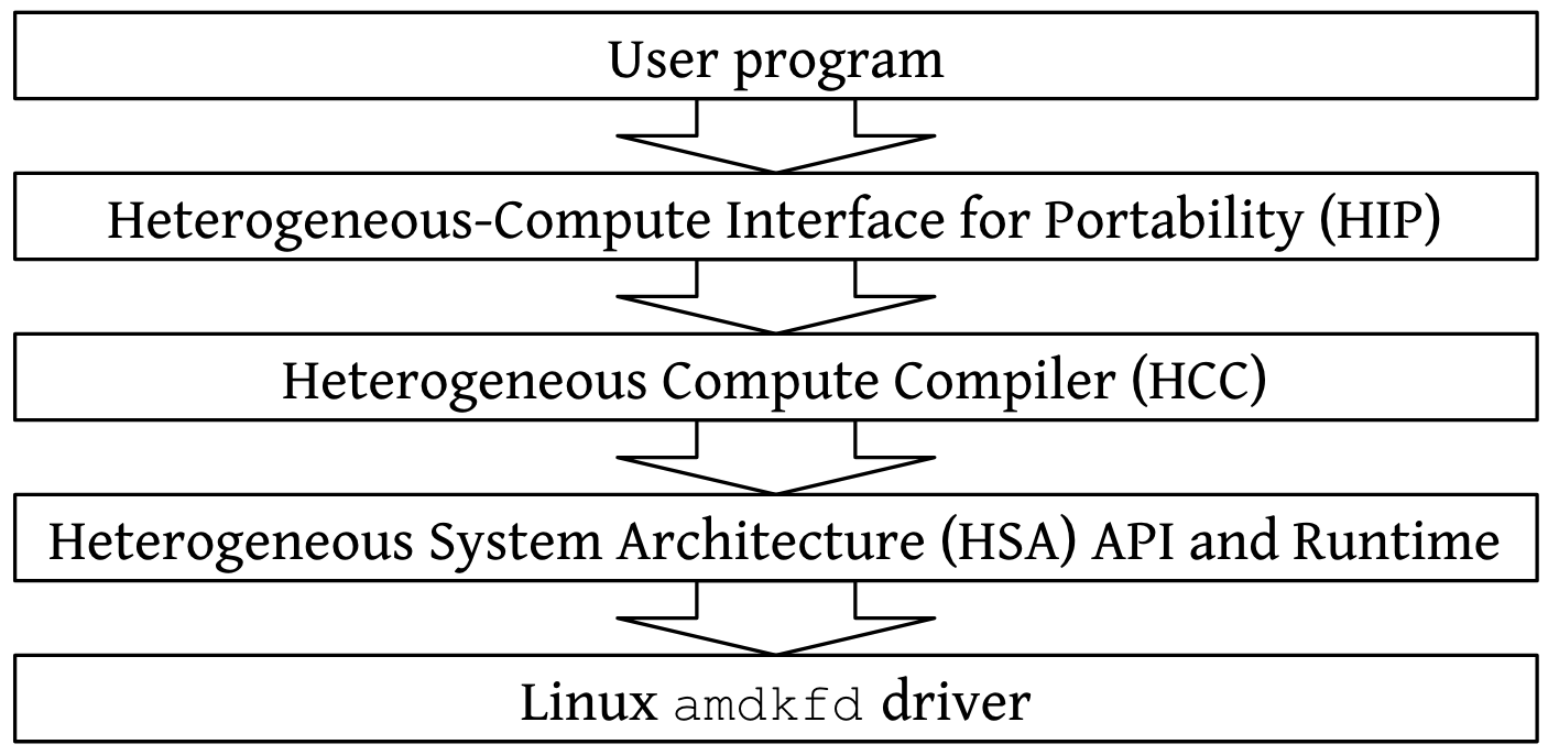
The above figure draws an overview of the software stack of AMD GPUs under Linux system 1. There are some basic yet confusing concepts when diving into the software stack. Here is a brief explanation to these items.
Compared to NVIDIA whose documentations are still opaque, AMD discloses many of their designs as well as hardware & software details. There are some useful docs available including but not limited to: RDNA & CDNA white papers and RDNA & AMD Intrinsic GPU ISA white paper. Here I’ll list some fundamental concepts when I went through these docs.
RDNA White Paper
RDNA architecture was proposed in 2019 and applied in the 7nm Navi GPU family including Radeon RX 5700 series. Compared to its predecessor GCN, AMD emphasizes on scalar architecture. Another difference is RDNA support wavefront with both 32 threads and 64 threads (called wave32 and wave64, respectively), while GCN only supports wave64 mode. Also, each CU in RDNA architecture now has 4 SIMD units, with each containing 32 ALUs, twice as the previous generation. Hence each SIMD unit is able to execute one whole instruction under the wave32 mode.
Now let’s dive into how the CU get organized:
 Here is the architecture of one CU in RDNA from the public slides. It contains:
- 4 32-lane SIMD units with corresponding VGPR (Vector General Purpose Registers).
- 4 scalar ALU with corresponding SGPR (Scalar General Purpose Registers).
- 2 L0 cache (newly-added cache hierarchy in RDNA), but they are not coherent.
- the 32 KB instruction cache and 16 KB constant cache shared between all SIMD units within the CU.
Besides, the CU obtains its new name WGP (Work Group Processor). As we discuss earlier, the 32-lane SIMD unit could execute 32-threads wavefront instructions natively (in 1 cycle), while previous 16-lane SIMD has to execute one instruction from 64-threads wavefront in 4 cycles ().
 And 5 WGPs share the 128 KB L1 cache, while all WGPs share the global L2 cache and GDDR6.
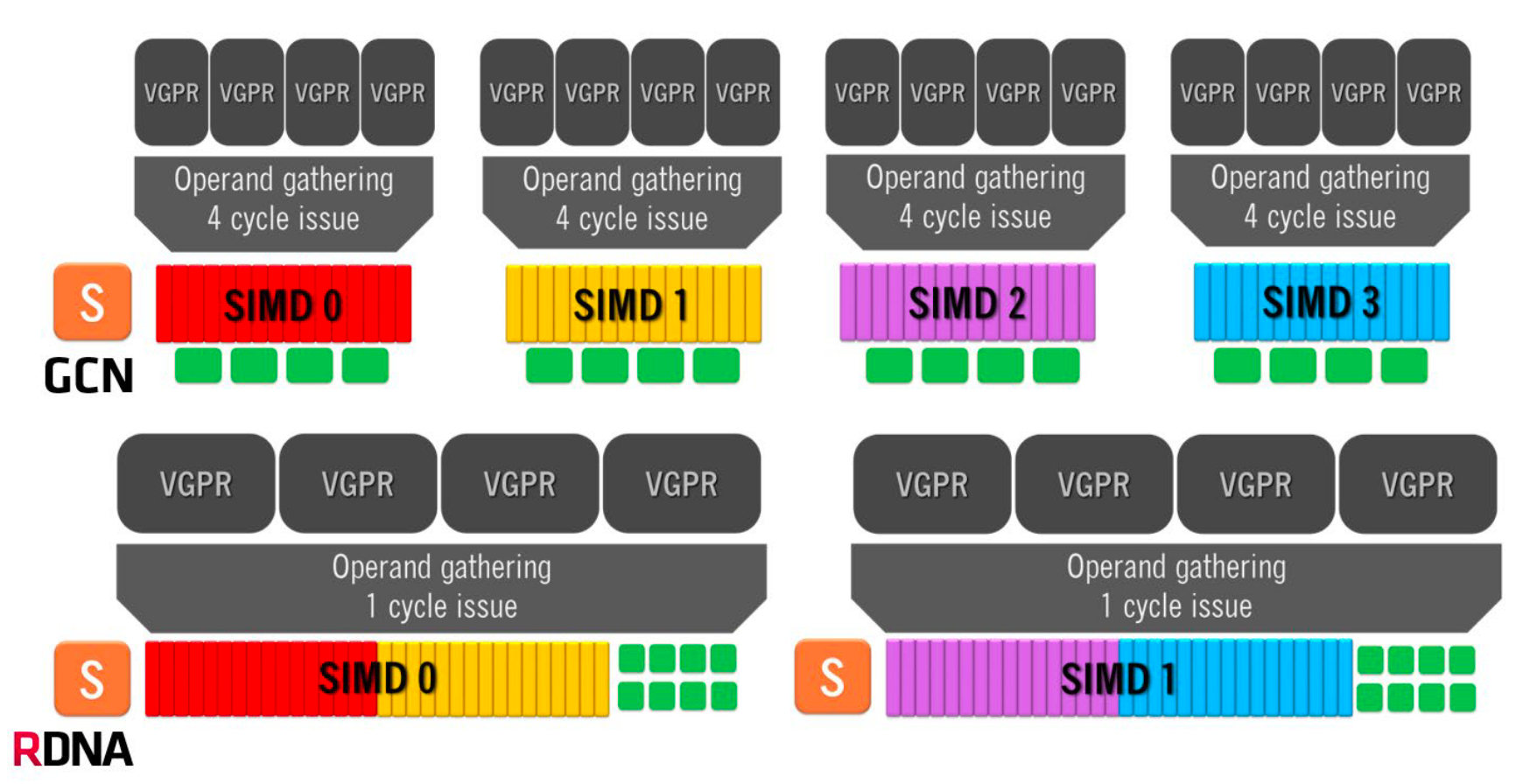 This figure from white paper help us compare the difference of instruction execution bewteen GCN and RDNA architecture. Each SIMD unit is extend as twice as the previous generation, thus each wavefront instruction could be executed in 1 cycle. To accomodate the narrower wavefront, the vector ALUs are also widened into 32-lane. Beyond this, the ALU also supports mixed-precesion FMA operation and dot-product among low-precision elements (
fp16, int8) stored in one register now.
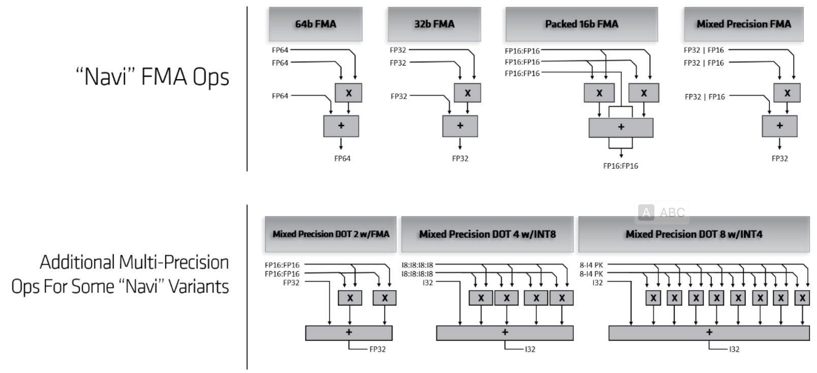 As for the double-precision calculation, there is one separate computing component in the vector ALU pipeline, which provides the opportunity for the overlapping of single-precision and double-precision computation. RDNA also adds cross-lane data paths for the efficiency of warp-level primitives (like shuffle or permutation).
Now let’s come to the newly-added L0 cache in the RDNA WGP. There are 2 L0 caches with each connecting a pair of SIMD units with memory bus. Each L0 vector cache is 16KB and 4-way set associative, with 128-byte cache lines to deliver a full wavefront of data every cycle. The L0 cache is write-through and uses an LRU replacement policy. While each L0 is coherent within a work-group, software must ensure coherency between the two L0 caches within a dual compute unit (how?). On a cache hit, the L0 cache will read out a 128-byte cache line and deliver the results back via the response bus.
L1 cache, as shared between several WGPs, is the next level in the cache hierarchy. Each L1 is 128KB with four banks and is 16-way set associative. The L1 cache is a read-only cache that is backed by the globally shared L2; a write to any line in the graphics L1 will invalidate that line and hit in the L2 or memory. There is an explicit bypass control mode so that shaders can avoid putting data in the graphics L1 (how?).
The L2 cache is shared across the whole chip and physically partitioned into multiple slices. The cache is 16-way set-associative and has been enhanced with larger 128-byte cache lines to match the typical wave32 memory request.
RDNA ISA
The RDNA ISA documents give us a more detailed introduction to the underlying hardware components, together with the RDNA instruction format and execution information.
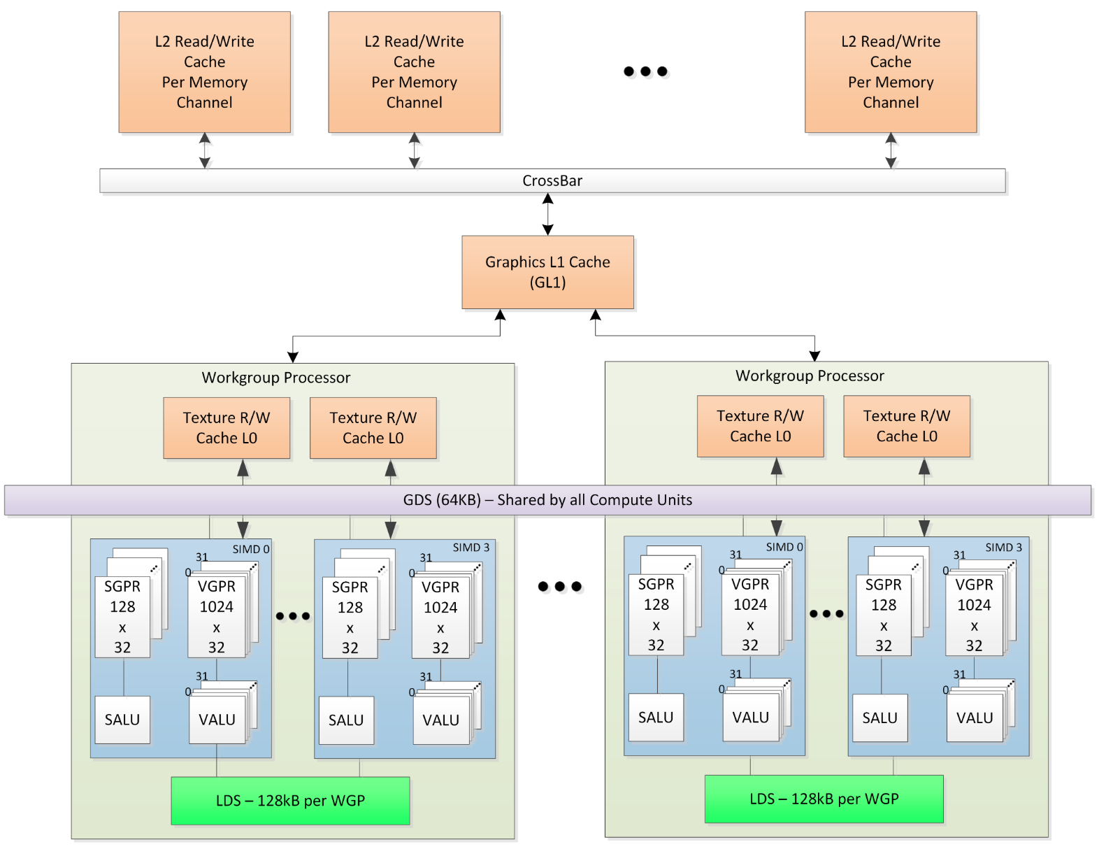
Here is a more straighforward overview of the memory system in the RDNA architecture from the ISA document. Except for the basic components we introduce aobve, the GDS (Global Data Sharing) component is a 64 KB software cache shared by all WGPs on the GPU. The GDS is configured with 32 banks, each with 512 entries of 4 bytes each. It can be used to store important control data structures need to be shared by all work groups (for example, control the execution order of each work group). It also contains dedicated atomic buffers.
Another findings is there are two configurable modes for LDS allocation: CU mode and WGP mode. Note that there are two CUs in each WGP, each with 2 SIMD units. The former mode splits the LDS into two parts and only allows data to be shared in half of wavefronts in the scheduled work group, and the other half of wavefronts can only use the other half of LDS meanwhile. Under the CU mode, wavefronts are scheduled to the CU connected to the corresponding half of LDS. The WGP mode, however, allows all wavefronts to access the entire LDS. The CU mode could be benefit from the parallel data accesses to the splited LDS but the data is less shared.
NaviSim is a good material for the architectural details of RDNA.
RDNA 2: 6900XT as Example, Compared to Ampere
AMD release the 2nd-RDNA top-tier gaming GPU in 2020, whose codename is “Navi 21” whatever. In this section, we are going to compare Navi 21 with its strong competitor: RTX 3080 (with NVIDIA Ampere arch.). Most figures in this section are borrored from2, and we may not focus on the graphic pipeline part.
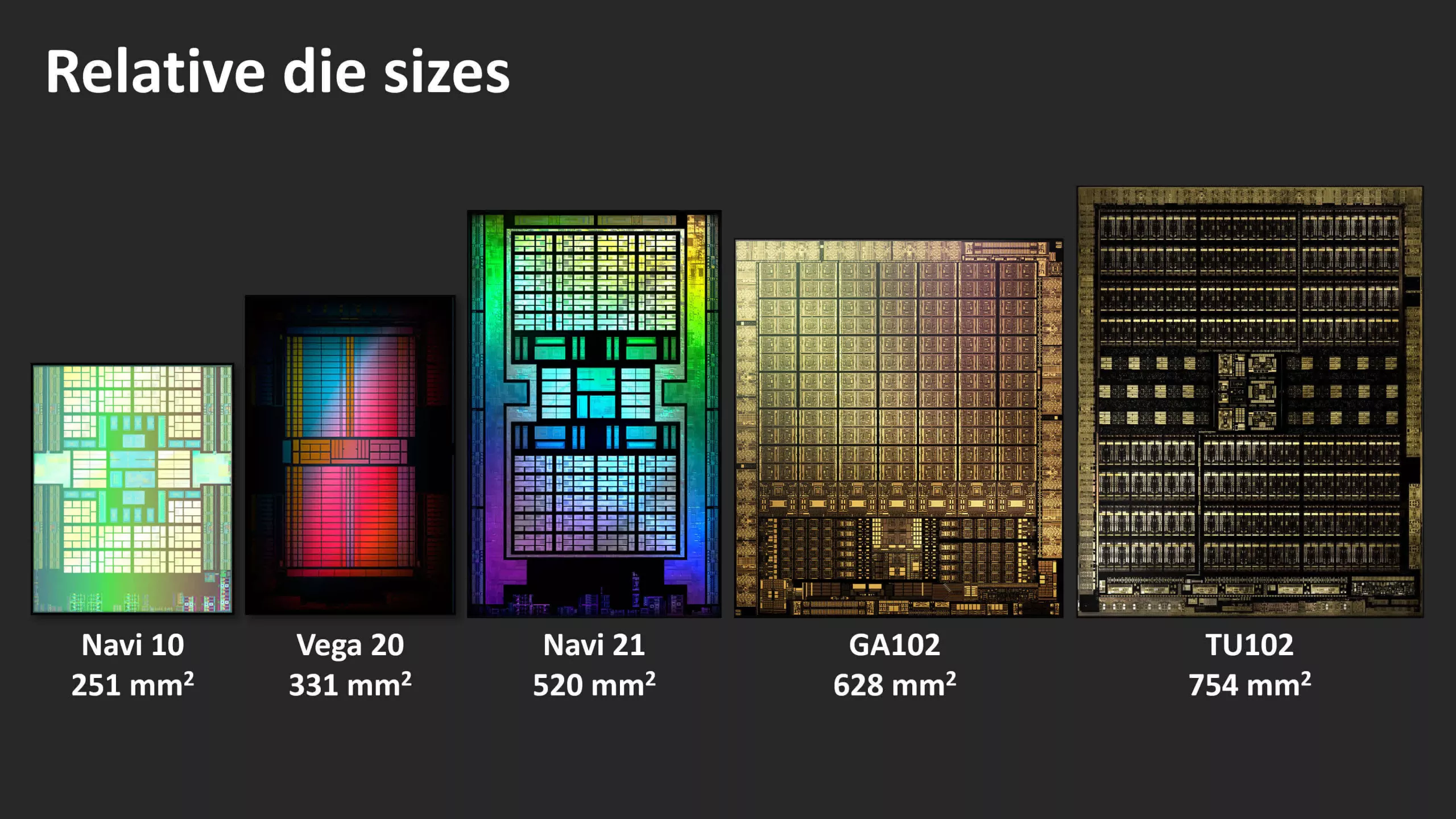
This is the die sizes comparison among different generations of GPUs from both NVIDIA and AMD. Note that Navi 21 is built on TSMC’s 7nm chip.
Both GPUs have a centralized command processor responsible for dispatching and managing operations targeting either graphics or computing workloads.
In AMD’s terminology, it’s called ACE (Async. Compute Engine), located in the center of chip.
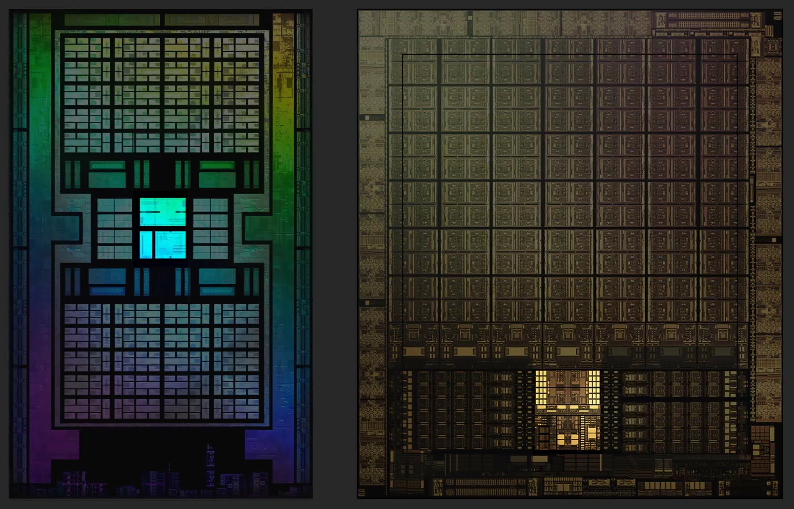 NVIDIA names it GigaThread Engine, but there are no public resources about it.
Let’s dive into the GPU hardware hierarchy, the first level is Graphic Processing Cluster (GPC, NVIDIA) or Shader Engine (SE, AMD):
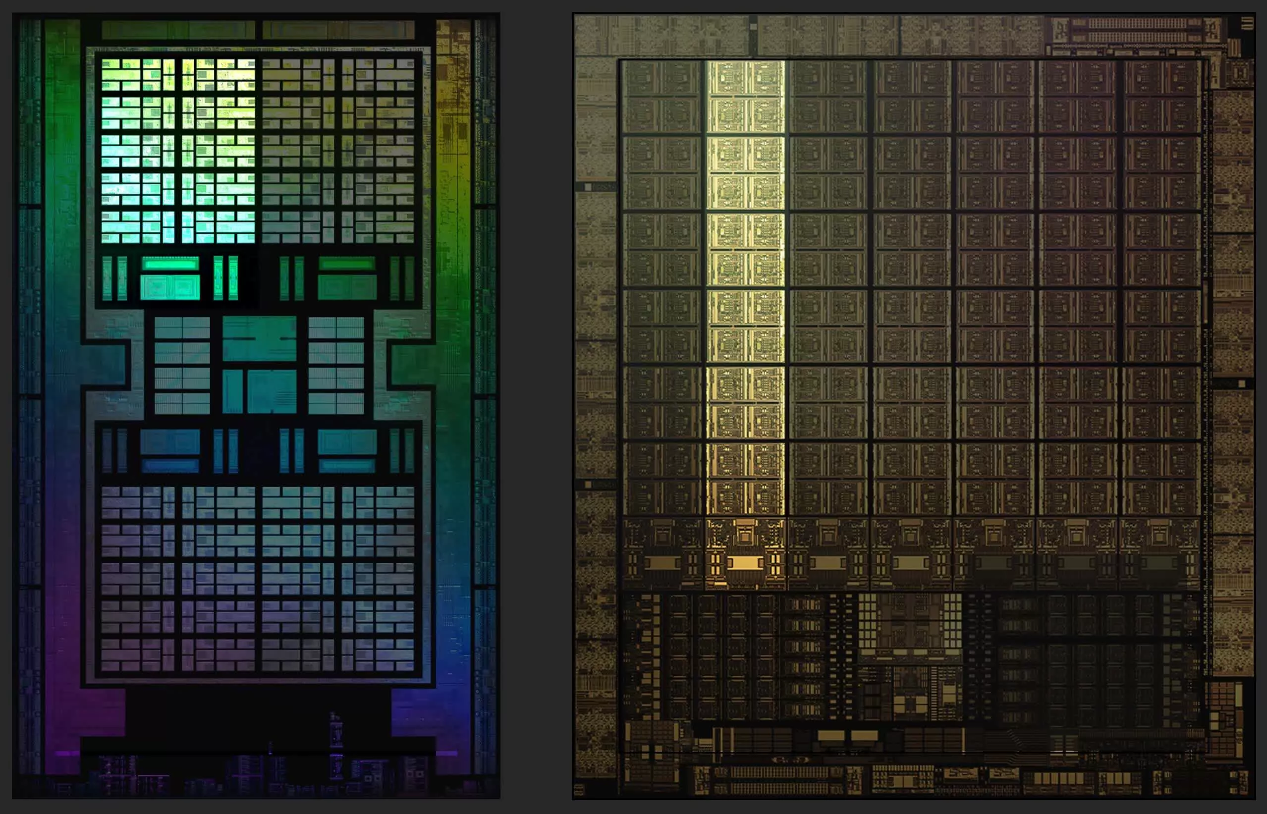 The central command processor offloads some of schedule responsibilities to the GPC or SE, and a number of SMs or CUs are grouped together into one.
In NVIDIA’s Hopper architecture, there is a newly-proposed relatively-transparent parallel hierachy: thread block cluster (TBC).
And CTAs inside one TBC will be dispatched to SMs across one GPC3.
But this is beyond our discussion.
In RDNA 2, two adjacent CUs are grouped as a new unit: Working Group Processor (WGP), also called DCU (Dual CU):
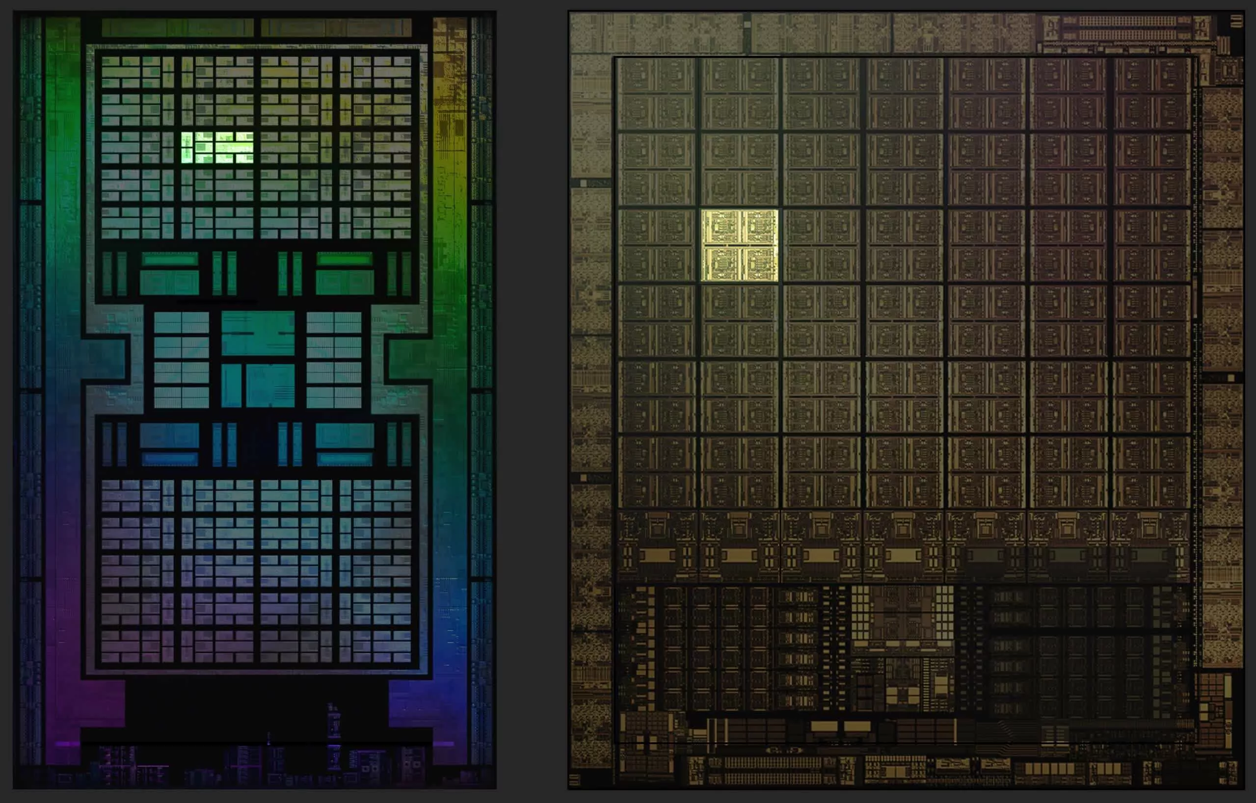
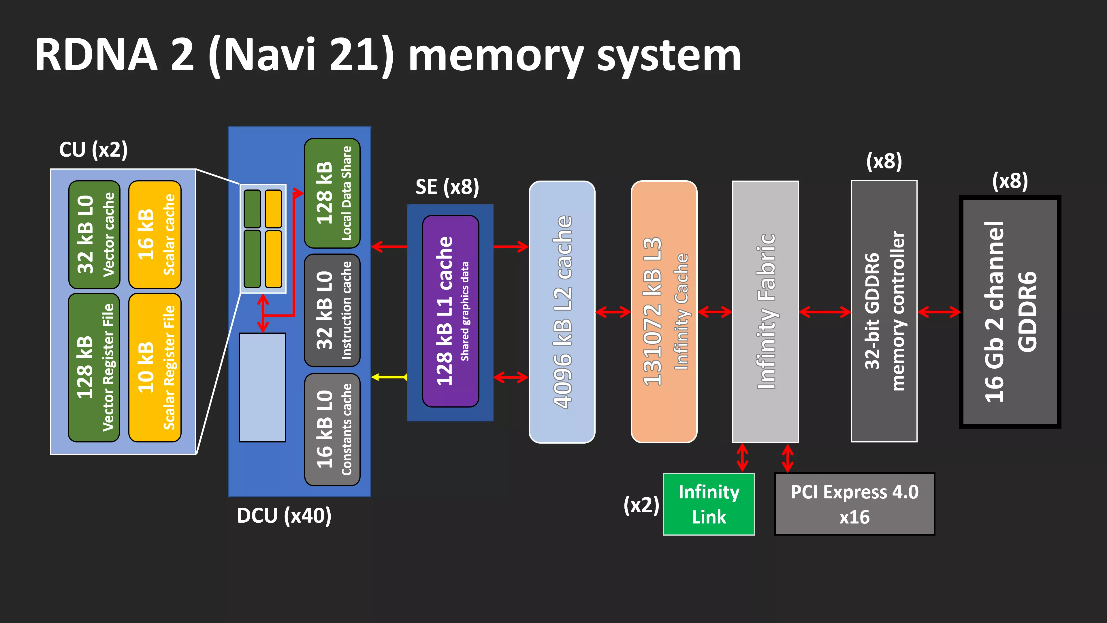
And the memory hierarchy corresponding to the newly-proposed DCU architecture.
One WGP (2 CUs) contains shared L0 cache as well as LDS. And 8 WGPs composes the shader engine, which holds the L1 cache.
The L2 and L3 cache are shared among all SEs and hence get their name “memory-side cache”.
CDNA White Paper
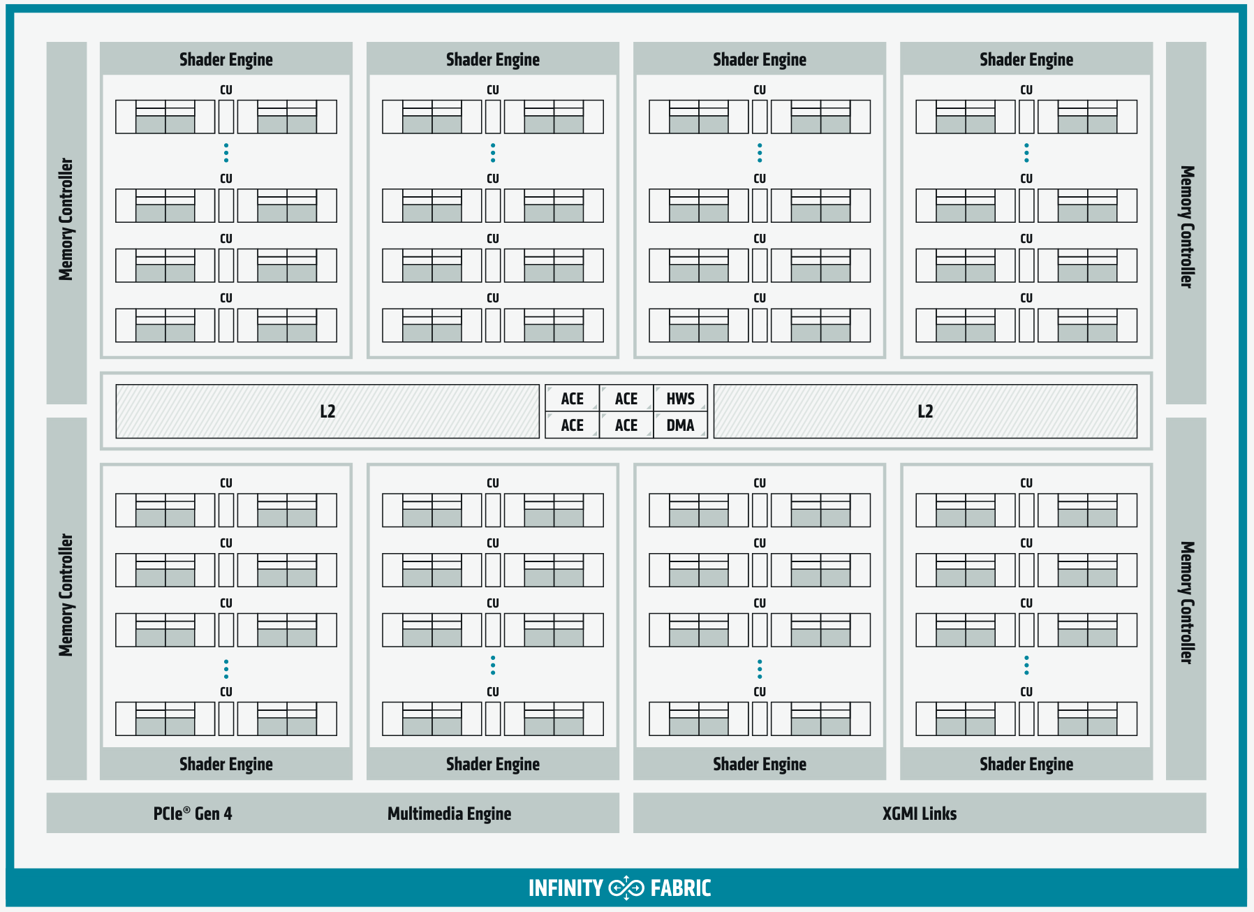 Here is the overview of the first incarnation of the AMD Intrinsic (CDNA 1) architecture. It should be noted that the CDNA architecture is built on the top of GCN, so the changes applied in RDNA has little affect on CDNA architecture. Though derived from GCN, the CDNA CUs are enhanced with Matrix Cores, analog to NVIDIA’s Tensor Core.
We left the CDNA 2 architecture as the following-up topic of this article.
Summary
- AMD GPU has 3 architecture codenames in gaming and graphic products since 2007: TeraScale, GCN and RDNA, with each codename having multiple generations.
- For the datacenter series, the architecture is CDNA (also called AMD Intrinsic), which is derived from the classic GCN architecture.
The table below is the comparison between analogical notations of NVIDIA and AMD:
| NVIDIA Notation | AMD Notation |
|---|---|
| SM (Streaming Multiprocessor | CU (Compute Unit) |
| Thread Block | Work Group |
| warp (32 threads) | wavefront (64 threads before RDNA, 32 or 64 threads since RDNA) |
| Shared Memory | LDS (Local Data Sharing) |
| Tensor Core | Matrix Core |
| NVLink | AMD Infinity Fabric |
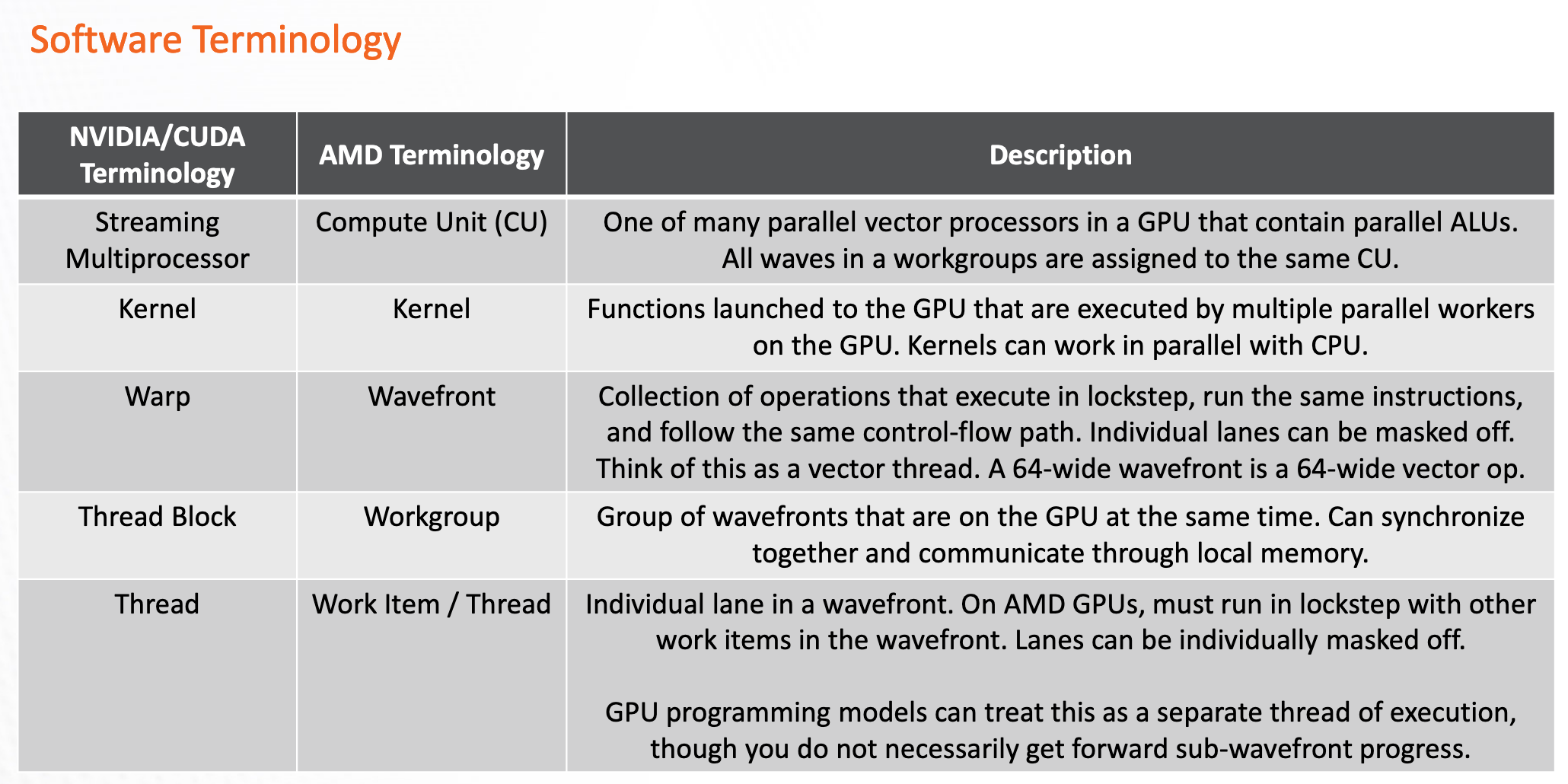
Here is another terminology comparison with description from4 :
References & Useful Links
There are some useful slides, documentations and articles public available online: architectural slides 1 5, slides 2 6.
Reading notes7 for the optimization guide5. AMD GPU Basics from ORNL4.
Footnotes
-
[ECRTS’20] AMD GPUs as an Alternative to NVIDIA for Supporting Real-Time Workloads ↩
-
https://forums.developer.nvidia.com/t/how-does-the-thread-block-cluster-of-the-nvidia-h100-work-concurrently/227962 ↩
-
# An Architectural Deep-Dive into AMD’s TeraScale, GCN & RDNA GPU Architectures ↩ ↩2
-
https://gpuopen.com/wp-content/uploads/2019/08/RDNA_Architecture_public.pdf ↩
-
https://interplayoflight.wordpress.com/2020/05/23/optimizing-for-the-rdna-architecture-presentation-notes/ ↩